New paper in Nature Photonics on attosecond-fast internal photoemission

Charge separation at an interface between two materials is a fundamental process in electronic components. It determines how fast signals can be transmitted in transistors and how efficiently power is generated in solar cells. Novel material combinations of stacked two-dimensional materials, so-called heterostructures, allow such interfaces to be tailored on the atomic scale.
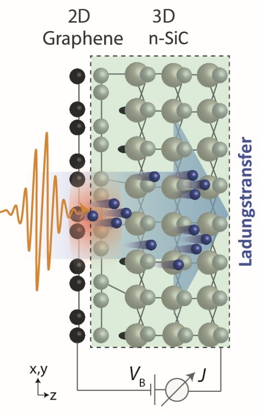
In order to investigate how fast charge transfer takes place at such an interface, we have epitaxially grown a monolayer graphene, an atomic thin film of carbon atoms, on top of the doped semiconductor silicon carbide (SiC), in collaboration with our colleagues from Applied Physics (Prof. Dr. Heiko B. Weber). Such an interface of a metal and semiconductor is known as Schottky contact. In contrast to ordinary Schottky contacts, which are equipped with metal electrodes, graphene offers the advantage that the electrons can be excited with a laser field. These excited electrons only have to travel atomic distances to reach the silicon carbide (see figure). As a result, this charge transfer could be extremely fast – ultrafast on the femto to attosecond time scale. Such fast charge transfer has the potential to enable clock rates in the range of petahertz (1015 Hz), and thus to operate more than a thousand times faster than today’s electronic components. Until now, however, there has been a lack of methods to measure charge transfer times in the attosecond range.
We have optically investigated the charge transfer time from graphene to SiC. For this purpose, we have developed a new method, which we have named CHAMELEON: charge transfer time measurement via laser pulse duration-dependent saturation fluence determination. CHAMELEON is based on the fact that we use saturable absorption in graphene as an internal ultrafast clock.
For 6 femtosecond laser pulses, the excitation of electrons from the valence band to the conduction band saturates for a certain fluence (number of photons). The exact value of the saturation fluence depends on how fast electrons leave graphene during the laser pulse excitation: Some of the electrons go back to the valence band, but some of the electrons go from the graphene to SiC via the material interface. If we stretch the laser pulses in time while maintaining the number of photons in the pulse, more electrons can be discharged during the laser pulse duration. Thus, a higher fluence is required to achieve saturation of the excitation. By measuring the saturation fluence as a function of the laser pulse length, we can therefore obtain the charge transfer time from graphene to SiC.
Since the electric field between graphene and SiC can be varied by applying a reverse voltage, the charge transfer times we measured are in the range of (210 ± 80) femtoseconds for a small applied voltage and go down to 292 ± 210 attoseconds for the largest applied voltage. 292 attoseconds represents the fastest charge transfer time ever measured at a material interface, which is also relevant for current and future electronics.
Our contribution has just been published in Nature Photonics. The press release of the Friedrich-Alexander university can be found here.