Accelerator on a Chip International Program — ACHIP
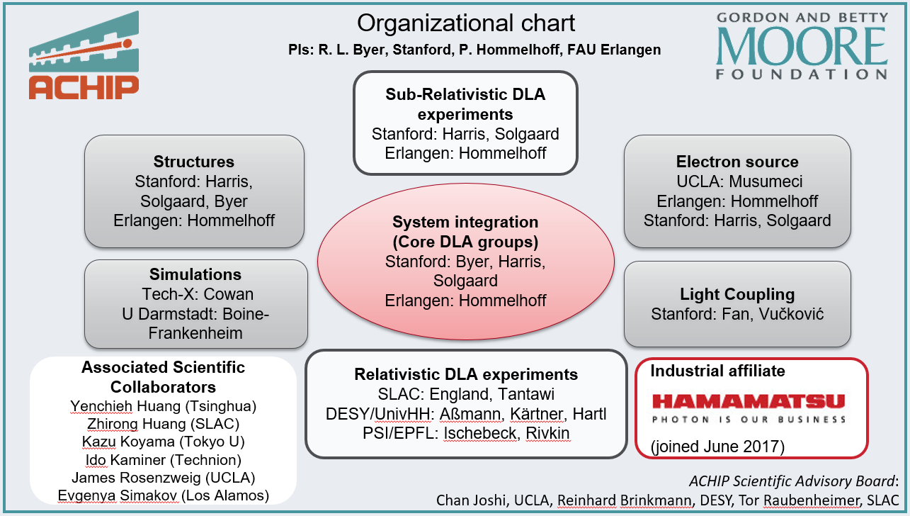
ACHIP, with a total of $20 million generously funded by the Gordon and Betty Moore Foundation from November 2015 through 2024, is headed by Stanford University and our group at FAU. See here for the Stanford ACHIP web site. Next to Stanford and FAU, the following groups were members of ACHIP:
DESY (R. Assmann, I. Hartl)
EPFL (L. Rivkin)
Hamburg University (F. Kaertner)
PSI (R. Ischebeck)
Purdue University (M. Qi)
SLAC (J. England, S. Tantawi)
Stanford University (B. Byer, S. Fan, J. Harris, O. Solgaard, J. Vuckovic)
Tech-X (B. Cowan)
TU Darmstadt (O. Boine-Frankenheim)
UCLA (P. Musumeci)
Industrial affiliate: Hamamatsu Photonics
On this page, we show example results from ACHIP research, but continue the reporting with work after ACHIP had ended. The outstanding success of ACHIP becomes clear with the two final highlight papers both demonstrating an accelerator on a chip: the Stanford/Darmstadt work published in PRL, and the Erlangen work published in Nature. The echo was tremendous, see here.
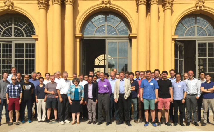
The members of the Accelerator on a Chip International Program, ACHIP (Erlangen, 2016)
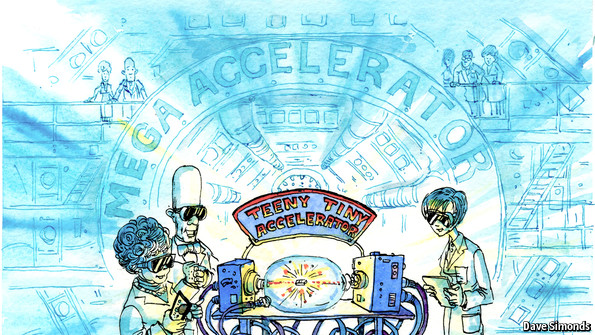
Accelerators on a chip: Dielectric laser accelerators
Particle accelerators are exciting research tools that provide energetic high brightness charged particle beams that can be used to probe physical phenomena otherwise inaccessible. However, the enormous cost and user demand of many of the radio-frequency based accelerators limits their availability. To provide an accelerator accessible on the university-lab scale, a novel accelerator design must be developed.
One such design, whose development is funded by the Gordon and Betty Moore Foundation (press release), is the Dielectric Laser Accelerator or DLA for short. DLAs leverage both the GV/m electromagnetic fields of commercially available lasers and the advanced nanofabrication techniques of dielectric materials developed in the semiconductor industry. The large available electromagnetic fields are used to create acceleration gradients that exceed those in radio frequency accelerators by a factor of 100. Even though DLAs are orders of magnitude smaller than their RF brethren, their accelerating gradients allow for DLAs to impart similar energy gains to charged particles. However, instead of imparting these energy gains over meters, DLAs impart these energy gains over millimeters, potentially enabling a university lab-scale particle accelerator.
The DLAs tested at FAU operate in a phase-synchronous scheme, as follows. An incident laser pulse impinges upon a nanofabricated accelerating structure, exciting travelling near-field modes. Electrons, propagating in close proximity to the structure, are accelerated when their velocity matches the phase velocity of one of the traveling modes, and they are injected into these fields at a particular time. This synchronicity condition and general principle is similar to that employed in large-scale RF accelerators, and the structures are designed to satisfy this condition (see video produced by our SLAC partners on the dual-grating approach).
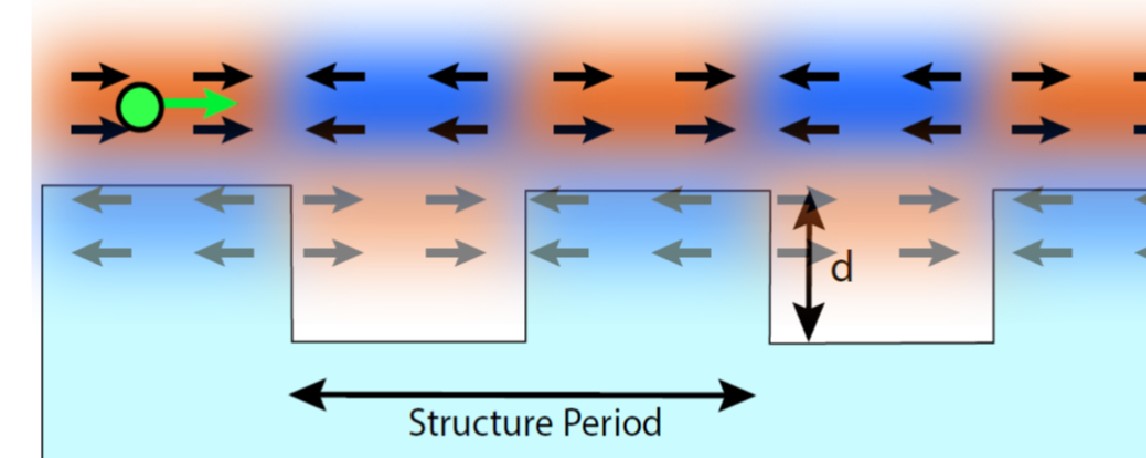
A laser impinges upon the silicon grating (with the structural period and grating height d indictated) from above, exciting the travelling wave mode depicted by the blue and red regions in the bottom image that shows a cross section of two periods of the accelerator. An electron, depicted by the green circle and travelling to the right, surfs the travelling wave, also moving to the right. (Image: FAU/Joshua McNeur)
Already there have been repeated confirmations that this principle of acceleration works over a wide range of electron velocities (from 15% to 100% of the speed of light) and lasers [1,2,3,4]. The ACHIP collaboration, see below, aims to extend the success of DLAs towards the realization of the analogy of an accelerator beamline. Multiple stages of dielectric-laser based acceleration, focusing, and diagnostics are being developed and tested. Specifically, auxiliary dielectric elements can be integrated [4,5] to additionally provide spatial focusing, steering, and bunching of electron pulses, important elements making up an essential toolbox in any particle accelerator.
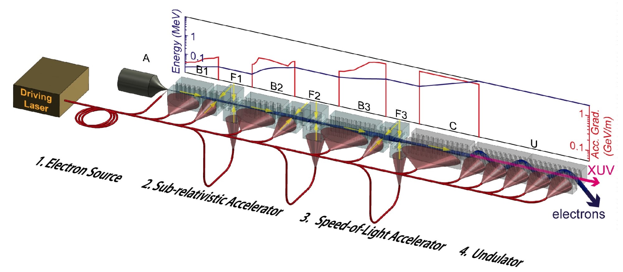
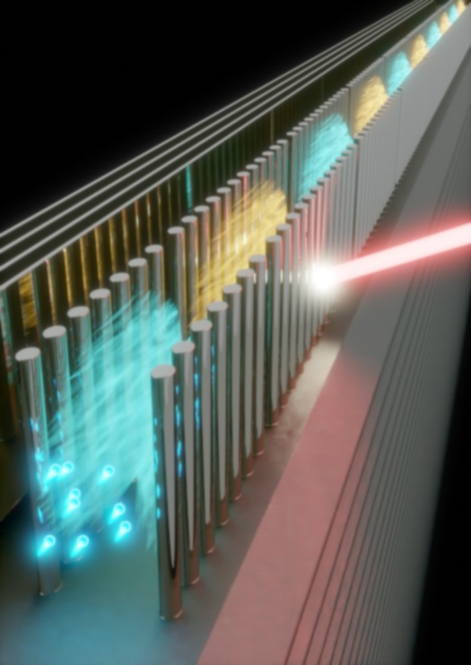
A laser-triggered electron cathode appropriate for operation with DLAs will eventually be incorporated with the multiple stages, resulting in a beamline where electrons are generated via laser-triggered emission, and then alternatingly accelerated, collimated, and diagnosed with sequential DLA-based devices. The complete accelerator can be schematically illustrated as shown below:
The resulting beam may be used as a high brightness light source via the incorporation of an element that wiggles the electron beam transverse to its direction of motion, creating photons as the beam alternatingly curves upwards and downwards. The compact size of such a beamline and its various components allows for many exciting applications, ranging from handheld MeV electron sources for tumor irradiation to table-top Free Electron Lasers [8].
Driving the accelerator
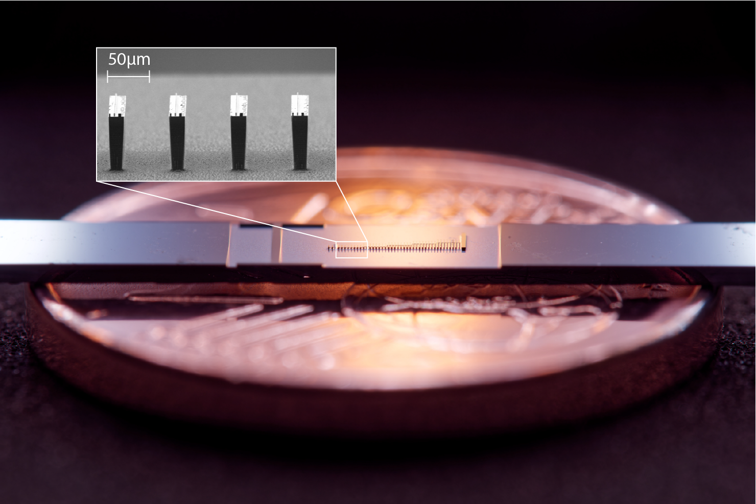
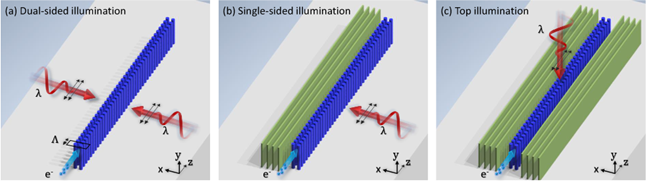
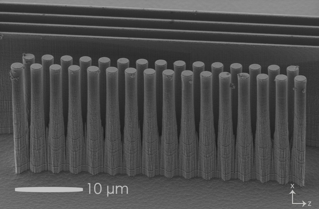
There are various schemes for generating the laser-induced accelerating field in the nanostructure. The structures, which consist of two rows of silicon pillars, can be illuminated by two laser pulses arriving at both sides of the structure.
We have previously shown that by adding a distributed Bragg reflector (DBR) to one side of the structure, it is possible to efficiently drive the structure with only one laser pulse. The DBR reflects the incoming light, which interferes constructively inside the structure, leading to an enhanced acceleration field. We could demonstrate an acceleration gradient of 133 MeV/m with these structures.
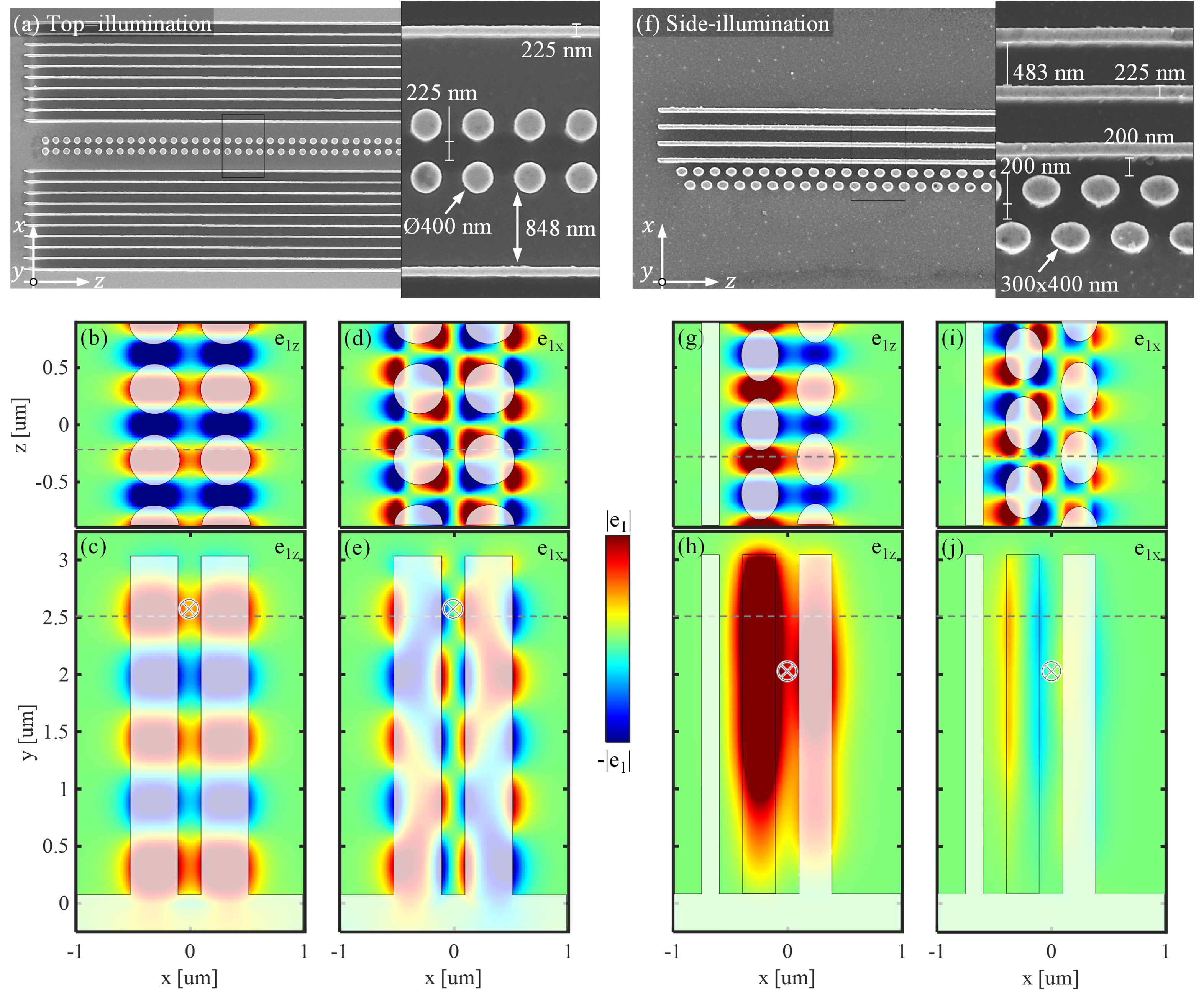
More recently, we have investigated the possibility of illuminating the structure from the top, perpendicular to the chip surface. (https://opg.optica.org/oe/fulltext.cfm?uri=oe-29-10-14403&id=450508) This approach greatly simplifies the experimental procedure, as it is no longer necessary to precisely align the laser beam (or even two beams) to the only micrometer-tall structure from the side. Additionally, since the field is no longer invariant in the vertical direction, this could open the possibility of vertical beam confinement in the structure.
Phase space dynamics and control in dielectric laser accelerators
Future technologies necessary to drive forward the development of dielectric laser accelerators require precise control of the phase space the electrons occupy.
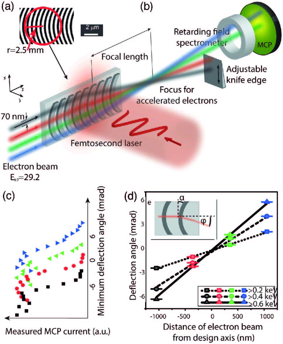
One avenue toward this is to modulate the longitudinal phase-space via ballistic bunching. In a first interaction (red), a sinusoidal energy modulation is imprinted on the electrons. Since the electrons are not relativistic (1/3 of the speed of light in our experiments), the difference in speed of individual electrons causes them to bunch in space during a defined drift distance. This causes the formation of a train of microbunched electrons. The longitudinal density modulation is probed via a second interaction (blue). There, the electrons experience a phase dependent energy modulation. Combined with realistic numerical models, this allows us to retrieve the density distribution of the electrons, or in other words – the microbunch length.
Short microbunches are necessary to inject electrons at a precise phase into phase sensitive DLA devices using, for example, alternating phase focusing (APF). These short electron pulses – in the range of roughly a hundred attoseconds, are furthermore interesting tools for ultrafast physics, to probe, for example, electronic states in condensed matter physics.
Alternating Phase Focusing (APF)
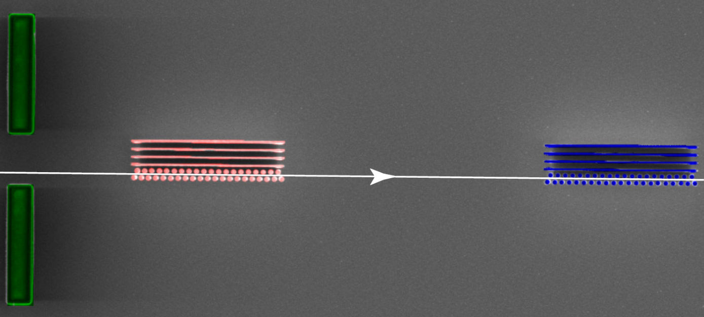
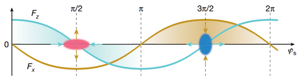
While dielectric laser accelerators are evolving from initial demonstration experiments into a viable accelerator technology, the challenges of designing such an accelerator are becoming increasingly apparent. One problem with the acceleration of a particle beam is the constant defocusing in the transverse direction. In classical accelerators, this is counteracted, by constantly refocusing the beam, either through external quadrupoles or by focusing modes in the accelerator itself. The experimental demonstration of electron beam focusing with a curved dielectric grating [5] opened up the possibility of applying some of these techniques to dielectric laser accelerators. The theoretical research into new focusing methods for DLA is being pursued at the TU Darmstadt. In simulation, the group led by Uwe Niedermayer was able to develop an implementation of alternating phase focusing in dielectric laser accelerators, a well-known technique in classical particle accelerators. In our joint publication [8], we present the theoretical work on how to accelerate an electron beam from 83 keV to 1MeV while simultaneously allowing most of the electrons to reach the end of the structure. The experimental demonstration of APF for guiding of electrons in a very small channel has now been shown for a 77 long structure [13]. In short, the phase relation between the electron and the electromagnetic field in the structure is changed (see figure) by briefly increasing the distance between the otherwise periodic columns. Thus, at approximately the same speed, the electron arrives in the structure at a different time or amplitude of the electromagnetic wave, so that the force also changes between positive and negative transverse directions. This ensures that when the electron is in one section in between the pillars, it is focused into the channel, and then in the next section, when it is focused too strongly into the channel, the force is reversed and the electron is defocused again towards the edge of the structure. In the constant alternation of forces, the electron beam can thus be guided through a narrow channel. These experiments are the first step for coherent acceleration of electrons in nanophotonic structures, where the electrons are guided and accelerated simultaneously.
Coherent nanophotonic accleration
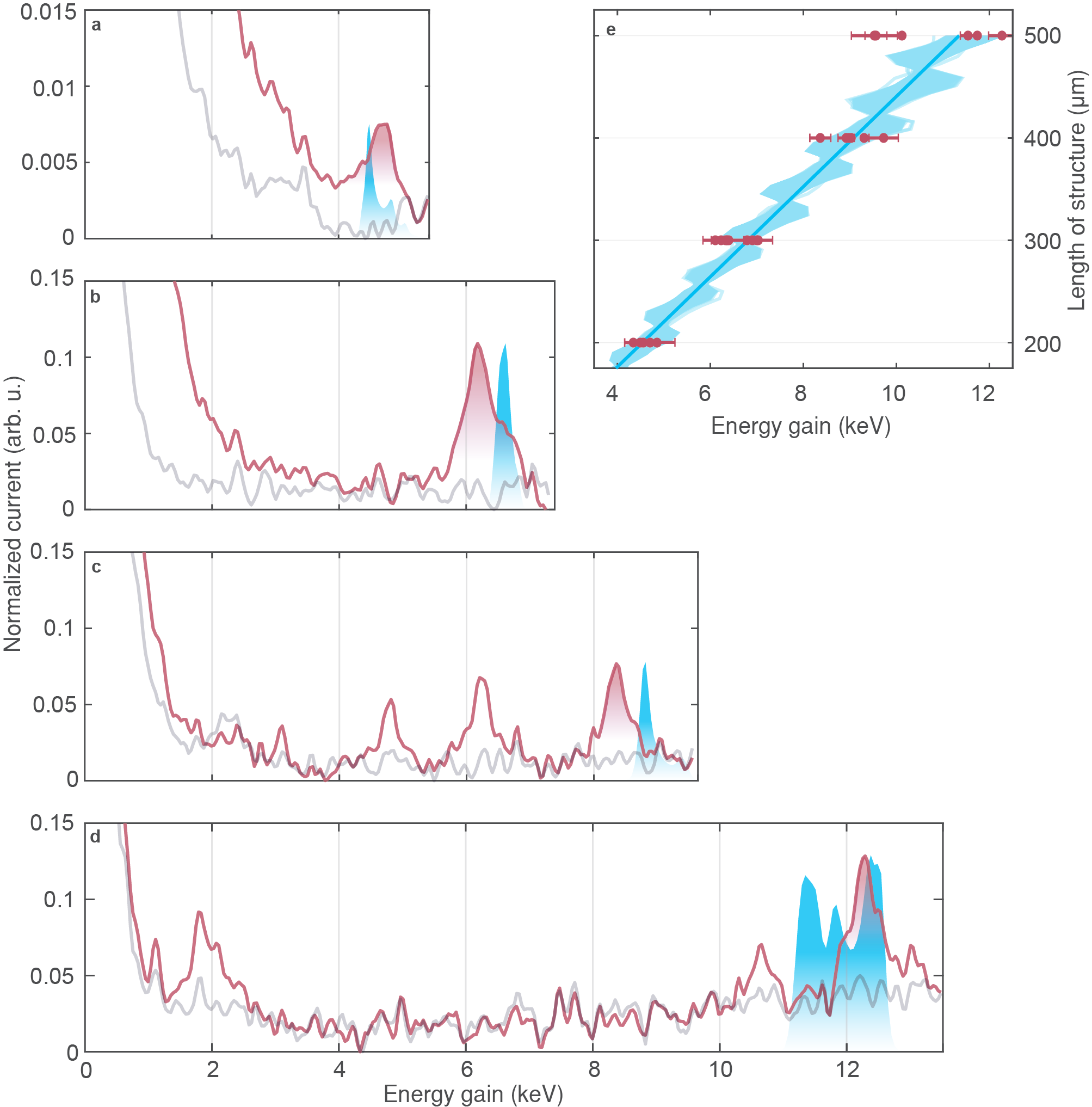
For coherent acceleration we “only” had to write the accelerating effect into the structure. This is achieved by switching the phase between points with the focusing and defocusing effect, and net acceleration. In this way, we were able to guide electrons through an accelerating channel up to 0.5 mm long and only 225 nm narrow, increasing the starting energy from 28.4 keV to 40.7 keV. The relative energy gain is thus 44% and the electron energy gradient is 22.7 MeV/m [14]. The data can be seen in the figure below.
Exploring longer wavelengths
Despite significant advancements, several challenges hinder the practical implementation of DLAs. These include low current transmission and strict requirements on electron beams due to the narrow channel widths, as well as fabrication challenges due to the small dimensions. Additionally, the damage threshold of the structure material limits the achievable acceleration gradient. Increasing the excitation wavelength from the typically used near-infrared (around 2 micrometers) to the mid-infrared could address these issues by allowing larger structure periodicities and channel widths, facilitating higher transmission and easier fabrication, as well as allowing for higher input fields due to the expected larger damage threshold.
In collaboration with the Fraunhofer Institute in Jena, we have designed and tested a silicon DLA structure for 10 micrometer excitation wavelength. The structure demonstrated an acceleration gradient of 93 MeV/m, comparable to near-infrared DLAs. The damage threshold of the pillars was found to be at least 5.2 GV/m, an order of magnitude higher than in the near-infrared. This shows that mid-infrared DLA is a promising avenue for further development and could lead to a miniaturized accelerator that far outperforms today’s DLAs in gradient and accelerated current [15].
Nanocrystalline diamond-coated nanotips
The requirements of the electron source are very strict for dielectric accelerators. The geometry of the dielectric structures has direct consequences for the required beam quality of the electrons. To prevent the electrons from colliding with the structure, the beam size and divergence must be as small as possible (typically approx. 100 nm beam waist and 1 mrad divergence). In addition, the electron pulse duration should be shorter than the laser pulse duration (sub-ps) and the number of electrons per pulse should be as high as possible in order to accelerate as many electrons as possible. Because of these high demands on the electron source, we are also doing research on new electron sources that meet these requirements. A possible candidate is a tungsten tip coated with nanocrystalline diamond.
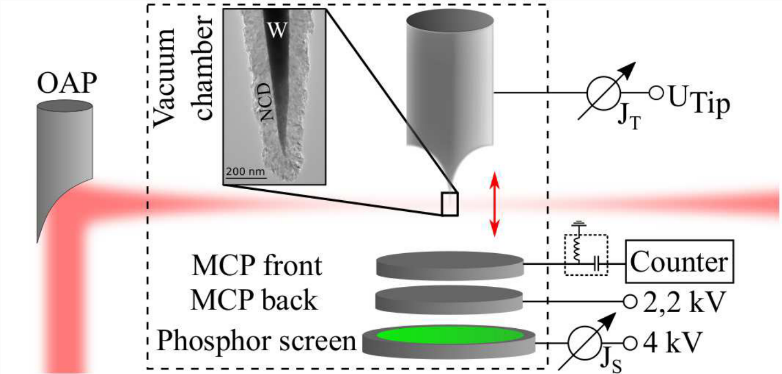
Diamond is a highly interesting material for electron sources because it is not only mechanically robust, chemically inert and thermally conductive, but also has a negative electron affinity – if the surface is saturated with hydrogen. Due to this special feature, diamond has a low work function and can show a significantly higher quantum efficiency than materials with positive electron affinity – i.e. almost any other materials. After fabrication and characterization [9] of diamond-coated tungsten tips, we also investigated the photoemission of electrons with ultrashort laser pulses [10]. The high photon density of femtosecond laser pulses allows efficient electron emission by multiphoton absorption. We measure the number of photons required per emitted electron at different wavelengths and can thus identify specific emission channels in the complex band diagram of the heterostructure.
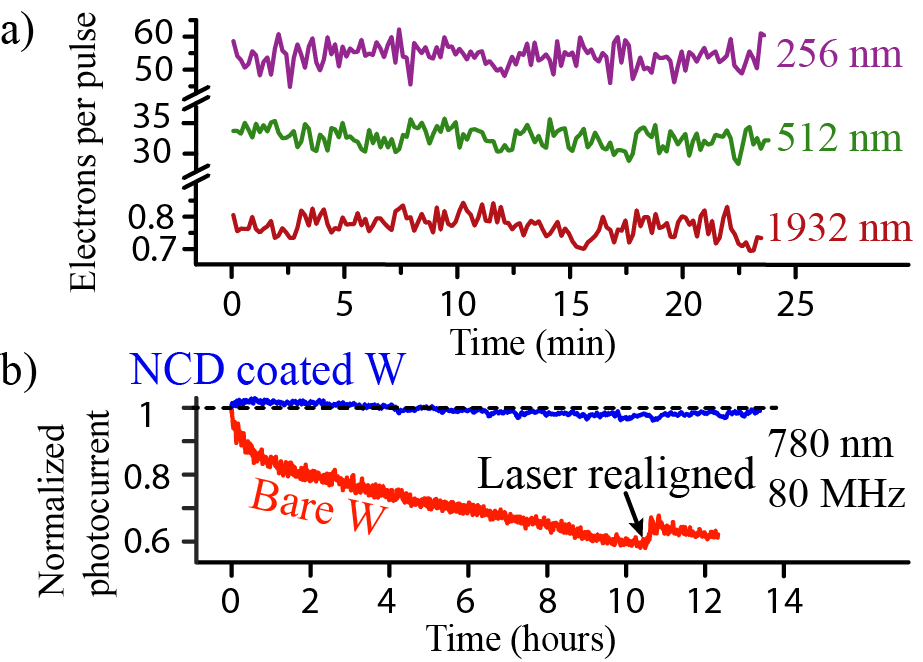
In addition, we characterize the potential application of these coated tips as ultrafast electron sources. We observe that the lower bound of the brightness is already comparable to the sources used today (e.g ultrafast SEM/TEM) and the stability is even better.
Ponderomotive interaction of laser fields and electron and attosecond electron pulse train generation
An alternative solution to electron pulse bunching using nanostructures involves the second-order all-optical ponderomotive scheme, in which two crossed laser beams generate an optical wave, either standing or co-propagating with the electron pulse. Free electrons impinging on such a transvers intensity grating will predominantly diffract as in the Kapitza-Dirac effect, or strongly disperse in a longitudinal grating [11]. In the latter case, a relatively long (~100 fs) electron pulse may be structured into a train of attosecond bunches with lengths below 300 as [12]. Such highly-bunched electron trains may be interesting not only for acceleration, but also for the ultrafast time-resolved probing of structural and chemical changes in atoms, molecules, and solids.
Very recently, we have achieved very similar results also in a nearfield scheme, so with the help of the photonic accelerator structures.
References:
Please find our full list of publications here.
[1] J. Breuer and P. Hommelhoff, “Laser-Based Acceleration of Nonrelativistic Electrons at a Dielectric Structure,” Physical Review Letters 111, 134803 (2013)
[2] E. A. Peralta, K. Soong, R. J. England, E. R. Colby, Z. Wu, B. Montazeri, C. McGuinness, J. McNeur, K. J. Leedle, Walz, E. B. Sozer, B. Cowan, B. Schwartz, G. Travish R. L. Byer, “Demonstration of Electron Acceleration in a Laser-Driven Dielectric Micro-Structure,” Nature 503, 7474 (2013).
[3] K. J. Leedle, A. Ceballos, H. Deng, O. Solgaard, R. Pease, R.L. Byer, J. Harris, “Dielectric Laser Acceleration of sub-100 keV Electrons with Silicon Dual Pillar grating Structures,” Optics Letters 40 18 (2015).
[4] J. McNeur, M. Kozak, D. Ehberger, N. Schönenberger, A. Tafel, A. Li, P. Hommelhoff, “A miniaturized electron source based on dielectric laser accelerator operation at higher spatial harmonics and a nanotip photoemitter” J. Phys. B: At. Mol. Opt. Phys. 49 034006 (2016).
[5] J. McNeur, M. Kozák, N. Schönenberger, K. J. Leedle, H. Deng, A. Ceballos, H. Hoogland, A. Ruehl, I. Hartl, R. Holzwarth, O. Solgaard, J. S. Harris, R. L. Byer, and P. Hommelhoff, “Elements of a dielectric laser accelerator,” Optica 5, 687-690 (2018).
[6] R. J. England, R. J. Noble, K. Bane, D.H. Dowell, C. Ng, J.E. Spencer, S. Tantawi, Z. Wu, R. L. Byer, E. Peralta, K. Soong, C. Chang, B. Montazeri, S.J. Wolf, B. Cowan, J. Dawson, W. Gai, P. Hommelhoff, Y. Huang, C. Jing, C. McGuiness, R. B. Palmer, B. Naranjo, J. Rosenzweig, G. Travish, A. Mizrahi, L. Schachter, C. Sears, G. R. Werner, R. B. Yoder. “Dielectric Laser Accelerators,” Rev. Mod. Phys. 86, 1337 (2014).
[7] P. Yousefi, N. Schönenberger, J. Mcneur, M. Kozák, U. Niedermayer, and P. Hommelhoff, “Dielectric laser electron acceleration in a dual pillar grating with a distributed Bragg reflector,” Opt. Lett. 44, 1520-1523 (2019).
[8] U. Niedermayer, T. Egenolf, O. Boine-Frankenheim, and P. Hommelhoff, „Alternating-Phase Focusing for Dielectric-Laser Acceleration“ ,Phys. Rev. Lett. 121, 214801, (2018).
[9] A. Tafel, M. Wu, E. Spiecker, P. Hommelhoff, J. Ristein, “Fabrication and structural characterization of diamond-coated tungsten tips,” Diamond and Related Materials, 97 107446 (2019).
[10] A. Tafel, S. Meier, J. Ristein, and P. Hommelhoff, “Femtosecond Laser-Induced Electron Emission from Nanodiamond-Coated Tungsten Needle Tips,” Phys. Rev. Lett. 123, 146802 (2019).
[11] M. Kozák, T. Eckstein, N. Schönenberger & P. Hommelhoff „Inelastic ponderomotive scattering of electrons at a high-intensity optical travelling wave in vacuum,“ Nat. Phys. 14, 121 (2017).
[12] M. Kozák, N. Schönenberger, and P. Hommelhoff, “Ponderomotive Generation and Detection of Attosecond Free-Electron Pulse Trains,”, Phys. Rev. Lett. 120, 103203 (2018).
[13] R. Shiloh, J. Illmer, T. Chlouba, P. Yousefi, N. Schoenenberger, U. Niedermayer, A. Mittelbach, and P. Hommelhoff, “Electron phase-space control in photonic chip-based particle acceleration” Nature 597, 498–502 (2021). https://doi.org/10.1038/s41586-021-03812-9
[14] T. Chlouba, R. Shiloh, S. Kraus, L. Brückner, J. Litzel and P. Hommelhoff, “Coherent nanophotonic electron accelerator” Nature 622, 476–480 (2023). https://doi.org/10.1038/s41586-023-06602-7
[15] L. Brückner, T. Chlouba, T. Morimoto, N. Schönenberger, T. Shibuya, T. Siefke, U. Zeitner and P. Hommelhoff, „Mid-infrared dielectric laser acceleration in a silicon dual pillar structure.“ Optics Express 32.16 (2024): 28348-28355
All pictures may be used if properly credited.
This publication can hardly be found online; we take the liberty of making the pdf available here: A. Lohmann, Electron Acceleration by Light Waves, IBM Technical Note 5, p. 169, 1962.